
design considerations for flex PCBs
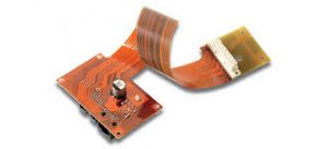
Flex circuits are a crucial element within modern electronic devices. They enable manufacturers to construct compact products that can conform to unique form factors, such as mobile phones and wearable gadgets. They also support innovative product designs by allowing designers to integrate both rigid and flexible elements in one single circuit board. The combination of rigid and flex sections enhances the durability of rigid-flex PCBs, making them suitable for use in applications that require resistance to mechanical stress and other environmental factors.
Incorporating manufacturability considerations into a flex pcb design is crucial for ensuring that it meets specific application requirements while enabling efficient manufacturing and assembly processes. This includes the selection of materials conducive to streamlined fabrication, as well as the implementation of optimized stiffener strategies.
Stiffeners are an essential component in the construction of a flex PCB, as they provide structural reinforcement and stability. Understanding the different types of stiffeners available and how to properly implement them in a design ensures that the resulting rigid-flex circuit board is capable of withstanding challenging operating conditions without compromising functionality or reliability.
What are the design considerations for flex PCBs?
Ensuring that conductive trace routing is compliant with specified bend radius guidelines prevents mechanical stress concentration points, which can degrade signal integrity. This is particularly important for flex PCBs that must be able to withstand significant bending or flexing operations.
Because flex circuits feature 2 coverlay layer files, they have a wider range of possible design configurations than 1-layer rigid boards. For example, it’s possible to include complex surface mount component placement patterns that would not be possible in a conventional single-layer rigid board design. Nonetheless, the size of these openings must be carefully controlled to prevent exposing unintended areas of copper or causing excessive shrinkage during the manufacturing process.
Because the etch yield and material strength of flex materials are lower, pad fillets are an effective way to improve etched pattern integrity. They are particularly useful for ensuring that the drill-to-copper distance is at least 8 mil, as this will allow for a higher etch rate and improved impedance control. However, they can be more expensive than the use of a standard hole.
The choice of panel plating or button plating is an important decision that should be made at the design stage. Panel plating results in a less dense metallization, which reduces the amount of copper needed for traces and vias. Button plating, on the other hand, allows for greater flexibility because the copper is only deposited on the vias/pads. It also results in more consistent traces and higher etch rates, but it may have a larger gap between pads, which could lead to signal losses.
For these and other important design considerations for flex PCBs, you should consult with your CM’s engineering team. They can provide expert advice on how to best design your rigid-flex PCBs for maximum performance and reliability.